Analytical electron microscopy is unique among material characterization techniques. It enables the examination of micro structural features through high-resolution imaging and the acquisition of elemental information from sub-micron regions of the specimen.
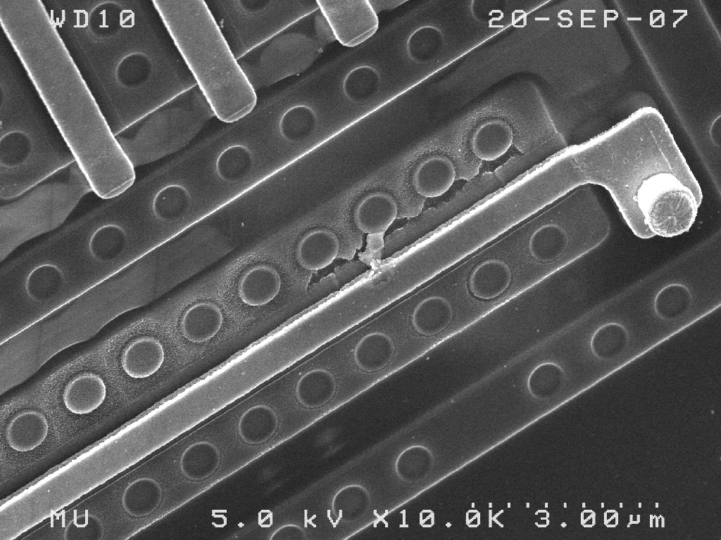
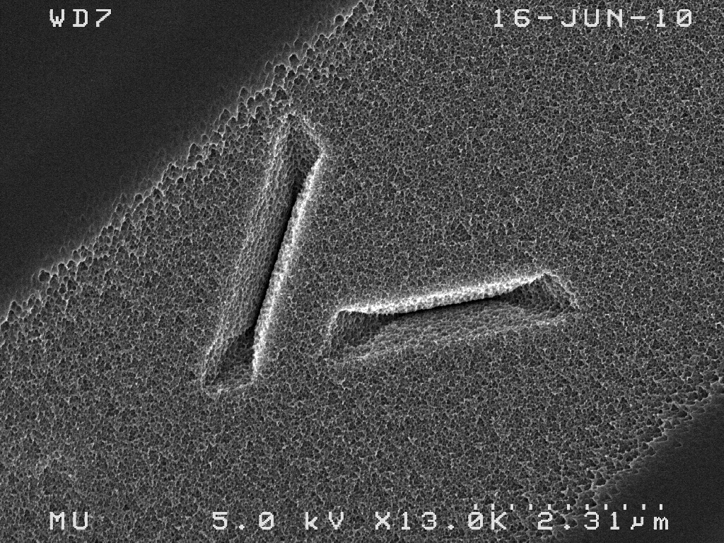
Another advantage of using electron beams is the increase in depth of field compared to optical microscopy. This allows clear pictures of complicated topological features.
The interaction of high-energy electrons with the sample produces X-rays, which can be analyzed spectroscopically to obtain elemental information about the specimen. Elements Na to U can be detected using our EDX detector.
Scanning Electron Microscopy (SEM) is a standard technique capable of imaging structures and materials at resolutions well beyond the limits of optical microscopy. The technique images surface topography with extreme depth of field.
FESEM with EDX
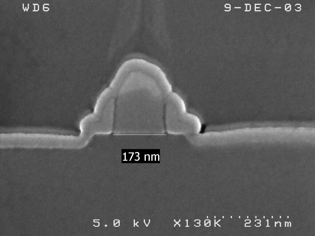
Gate of MOS transistor
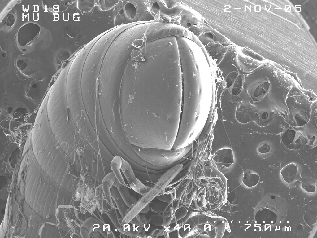
Insect